So, I have been trying to make this work, though I haven't been successful so
far, and I don't really think using pinctrl is a good solution for this either.
Comments inline.
On 04/14, Jonathan Cameron wrote:
> On Sat, 13 Apr 2024 12:33:54 -0500
> David Lechner <dlechner@xxxxxxxxxxxx> wrote:
>
> > On 4/13/24 11:14 AM, Jonathan Cameron wrote:
> > > On Tue, 9 Apr 2024 12:30:09 -0300
> > > Marcelo Schmitt <marcelo.schmitt1@xxxxxxxxx> wrote:
> > >
> > >> On 04/08, David Lechner wrote:
> > >>> On Mon, Apr 8, 2024 at 9:32 AM Marcelo Schmitt
> > >>> <marcelo.schmitt@xxxxxxxxxx> wrote:
> > >>>>
> >
> > ...
> >
...
> > >>>
> > >>> We identified A) an additional wiring configuration where SDI of the
> > >>> ADC chip is wired to SDO of the SPI controller and B) a potential need
> > >>> to pin mux between wiring modes to work around SPI controller
> > >>> limitations perhaps we could omit the adi,spi-mode property and just
> > >>> use the standard pinctrl properties.
> > >>>
> > >>> pinctrl-names:
> > >
> > > I'm lost on how pinctrl makes sense here.
> > > Yes you are changing the modes of the pins, but not in a conventional sense
> > > of some register that is being updated to say now use them like this.
> > > The mode is dependent on the timing sequence of how the pins are used.
> > > Otherwise looking at it a different way it's an external wiring thing we
> > > aren't controlling it at all. Is pinctrl suitable for that?
> > > I always thought of it as a way to change configurations of SoC pins.
> >
> > Yes, this is exactly what I think we need here.
> >
> > To write to the register, the chip has to be wired like this ("default"):
> >
> > +-------------+
> > +-----------------------------------| SDO |
> > | | |
> > | +--------------------| CS |
> > | v | |
> > | +--------------------+ | HOST |
> > | | CNV | | |
> > +--->| SDI AD7944 SDO |-------->| SDI |
> > | SCK | | |
> > +--------------------+ | |
> > ^ | |
> > +--------------------| SCLK |
> > +-------------+
> >
> > But to read sample data, the chip has to be wired in one of these
> > 3 configurations:
> >
> >
> > 3-wire mode ("single"):
> >
> > +-------------+
> > +--------------------| CS |
> > v | |
> > VIO +--------------------+ | HOST |
> > | | CNV | | |
> > +--->| SDI AD7944 SDO |-------->| SDI |
> > | SCK | | |
> > +--------------------+ | |
> > ^ | |
> > +--------------------| SCLK |
> > +-------------+
> >
3-wire mode like setup can be achieved if the SPI controller is capable of
keeping the ADC SDI line high (at VIO level) during ADC sampling, but keeping
controller SDO high throughout the entire transfer is not a thing all SPI
controllers can do (RPi's can't).
If the ADC is hard wired connected as in the 3-wire diagram then the user
can't write/read the configuration register. Same applies to "4-wire" mode
where controller CS is connected to ADC SDI.
The whole point of having pinctrl configurations was to make it possible
to both read/write config register and do ADC sampling if the SPI controller
can't keep ADC SDI at VIO. I don't think pinctrl can solve this problem though.
...
> >
> > If we want to be able to both write the register and read data,
> > some reconfiguration is needed. It might be possible to read data
> > using the register-write wiring configuration, but that only
> > works if SDO can be set to the correct state *before* the
> > CS line changes. This is not something that I think most SPI
> > controllers can do (e.g. Marcelo mentioned in the cover letter
> > that RPi always returns SDO to low after every xfer while
> > the AXI SPI Engine leaves SDO wherever it was last).
> >
> > >
> > > A pointer to some precendence in another driver for using it like this
> > > would go some way towards convincing me.
> > >
> > > Jonathan
> > >
> >
> >
> > I didn't find much precedence for something like this, but I
> > found devicetree/bindings/net/mediatek-bluetooth.txt that uses
> > pinctrl to pull a UART Rx pin low for a bootstrap mode which
> > sounds very similar to what we need to do here (pull the SPI
> > controller SDO pin high or low for 3-wire or chain mode).
> >
The pinctrl configuration for this ADC would not be meant to change once after
boot as it looks to be the usual use case for pinctrl (including mediatek-bluetooth.txt).
Also, no suitable mux for the "3-wire" mode in
Documentation/devicetree/bindings/pinctrl/xlnx,pinctrl-zynq.yaml
to do it like Documentation/devicetree/bindings/net/mediatek-bluetooth.txt.
The zynq pinctrl driver (drivers/pinctrl/pinctrl-zynq.c) would have to be
updated to add the new mux function in
static const struct zynq_pinmux_function zynq_pmux_functions[] = {
DEFINE_ZYNQ_PINMUX_FUNCTION(ethernet0, 1),
...
DEFINE_ZYNQ_PINMUX_FUNCTION(axi_spi_single, 1),
DEFINE_ZYNQ_PINMUX_FUNCTION(axi_spi_multi, 2),
though this is not really a thing that's on zynq, but one that is related to
these ADCs so I'm not sure it should go there.
> > For example, if we wanted to use 3-wire mode for reading
> > data, we would set the pinctrl to "default" to write the
> > register to configure the chip during driver probe. Then
> > to read data, we would change the pinctrl to "single" before
> > doing the SPI xfer to ensure that the ADC SDI pin is pulled
> > high independent of what the SDO line of the SPI controller
> > is currently doing.
No, the pin configuration for this ADCs would be expected to change unrestricted
amount of times. The pin configuration would have to change every time a sample
read is made after a register access transfers and vice-versa. If we decide
to support span compression, every change to _scale would lead to pinctrl
configuration change.
At pin level, we would want to rise SPI controller SDO line to VIO but then
the new SDO pin config would conflict with SPI pin group config.
I included pinctrl properties in my test dts to make use of pinctrl framework.
Yet, that doesn't really alternate SPI line configuration we are using because
the SPI function that is in the PS (FPGA's Processing System) is not what we are
interfacing when using spi-engine. Copy of my test dts at end of email.
Currently, the SPI controller we are using to test with these exotic ADCs
is the spi-engine which is implemented in the FPGA as an IP block which
owns control of the bus lines (SPI, SDO, CS, ...). To alternate the
configuration of SPI lines (pull SDO (ADC SDI) up to VIO, connect controller CS
to ADC SDI, etc.) I think it should be done in the HDL project. I don't think
it's a good idea to hijack spi-engine lines through pinctrl.
>
> Ah ok. This is implying that we are switching to a controllable
> mode to pull that pin high (or I guess one where it is always
> high). I'm not sure if that's more common than an SPI controller
> where you can set the 'don't' care state to high or low.
> I assume we can't get away with just setting the output buffer
> to all 1s because it won't hold that state between transfers?
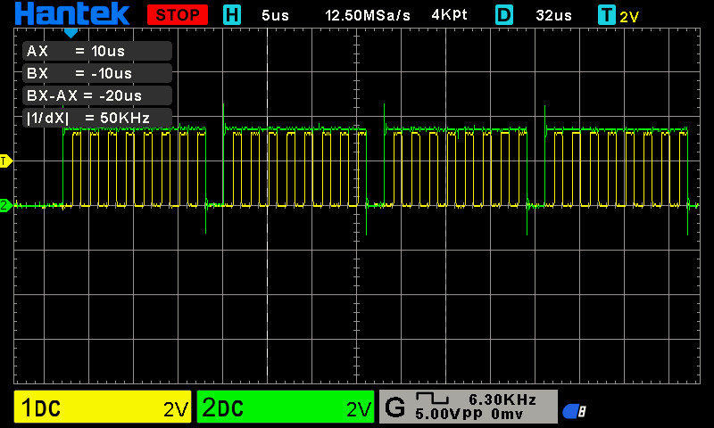
I tried sending the tx buffer filled with 1s when testing this with a RPi4 but
it brought the controller SDO (ADC SDI) line low between each 8 bits of transfer
(attaching an image (yellow line is SCLK, green lines is controller SDO)).
Anyway, can we have any guaranties with respect to controller SDO line behaviour
when its not clocking out data?
>
> Feels like that could be rolled into the SPI subsystem with
> any necessary transitions handled there (maybe)
To me, this sounds more reasonable than pinctrl.
Yeah, if we can set a don't' care state for the SDO line then that should be
enough for these ADCs.
Otherwise, can we really do anything if the controller can't keep SDO high?
>
> Just to check, this isn't just a case of a missing pull up
> resistor to drag that line correctly when it isn't actively
> driven (combined with all 1s in the write buffer) etc?
When using spi-engine, the controller SDO is connected to ADC SDI, controller
CS to ADC CNV and, for reg access, it works as conventional SPI.
spi-engine leaves the SDO line the state it was after last transfer so it we
can make it idle high during sample read. No hardware pull-up needed.
Marcelo
>
> Jonathan
>
>
The device tree source file I was using for testing with the ADC with the
changes for using pinctrl. Didn't really work.
// SPDX-License-Identifier: GPL-2.0
/*
* Analog Devices ADAQ4003
* https://wiki.analog.com/resources/tools-software/linux-drivers/iio-adc/ad400x
* https://wiki.analog.com/resources/eval/user-guides/ad400x
*
* hdl_project: <pulsar_adc_pmdz/zed>
* board_revision: <>
*
* Copyright (C) 2016-2023 Analog Devices Inc.
*/
/dts-v1/;
#include "zynq-zed.dtsi"
#include "zynq-zed-adv7511.dtsi"
#include <dt-bindings/pinctrl/pinctrl-zynq.h>
/ {
adc_vref: regulator-vref {
compatible = "regulator-fixed";
regulator-name = "EVAL 5V Vref";
regulator-min-microvolt = <5000000>;
regulator-max-microvolt = <5000000>;
regulator-always-on;
};
adc_vdd: regulator-vdd {
compatible = "regulator-fixed";
regulator-name = "Eval VDD supply";
regulator-min-microvolt = <1800000>;
regulator-max-microvolt = <1800000>;
regulator-always-on;
};
adc_vio: regulator-vio {
compatible = "regulator-fixed";
regulator-name = "Eval VIO supply";
regulator-min-microvolt = <3300000>;
regulator-max-microvolt = <3300000>;
regulator-always-on;
};
};
&pinctrl0 {
/* Restore conventional SPI pin configuration */
pinctrl_spi_default: default_config {
mux {
/* Are these the ones used by spi-engine? */
groups = "spi0_0_grp";
function = "spi0";
};
conf {
groups = "spi0_0_grp";
power-source = <IO_STANDARD_LVCMOS33>;
};
conf-spi-sdo {
pins = "MIO17"; /* SPI0 SDO? */
bias-disable;
};
};
/* Pull-up SPI SDO (ADC SDI) to VIO */
pinctrl_spi_single: single_config {
conf-spi-sdo {
pins = "MIO17"; /* Conflicts with SPI0 pin group */
bias-pull-up;
};
};
};
&fpga_axi {
rx_dma: rx-dmac@44a30000 {
compatible = "adi,axi-dmac-1.00.a";
reg = <0x44a30000 0x1000>;
#dma-cells = <1>;
interrupts = <0 57 IRQ_TYPE_LEVEL_HIGH>;
clocks = <&clkc 17>;
adi,channels {
#size-cells = <0>;
#address-cells = <1>;
dma-channel@0 {
reg = <0>;
adi,source-bus-width = <32>;
adi,source-bus-type = <1>;
adi,destination-bus-width = <64>;
adi,destination-bus-type = <0>;
};
};
};
axi_pwm_gen: axi-pwm-gen@ {
compatible = "adi,axi-pwmgen";
reg = <0x44b00000 0x1000>;
label = "cnv";
#pwm-cells = <2>;
clocks = <&spi_clk>;
};
spi_clk: axi-clkgen@44a70000 {
compatible = "adi,axi-clkgen-2.00.a";
reg = <0x44a70000 0x10000>;
#clock-cells = <0>;
clocks = <&clkc 15>, <&clkc 15>;
clock-names = "s_axi_aclk", "clkin1";
clock-output-names = "spi_clk";
};
axi_spi_engine_0: spi@44a00000 {
compatible = "adi,axi-spi-engine-1.00.a";
reg = <0x44a00000 0x1000>;
interrupt-parent = <&intc>;
interrupts = <0 56 IRQ_TYPE_LEVEL_HIGH>;
clocks = <&clkc 15 &spi_clk>;
clock-names = "s_axi_aclk", "spi_clk";
num-cs = <1>;
#address-cells = <0x1>;
#size-cells = <0x0>;
adaq4003: adc@0 {
compatible = "adi,adaq4003";
reg = <0>;
spi-max-frequency = <102000000>;
spi-cpha;
pinctrl-names = "default", "single";
pinctrl-0 = <&pinctrl_spi_default>;
pinctrl-1 = <&pinctrl_spi_single>;
vdd-supply = <&adc_vdd>;
vio-supply = <&adc_vio>;
ref-supply = <&adc_vref>;
adi,high-z-input;
adi,gain-milli = <454>;
};
};
};
Attachment:
dso_01_01_00_34_00.jpg
Description: JPEG image
