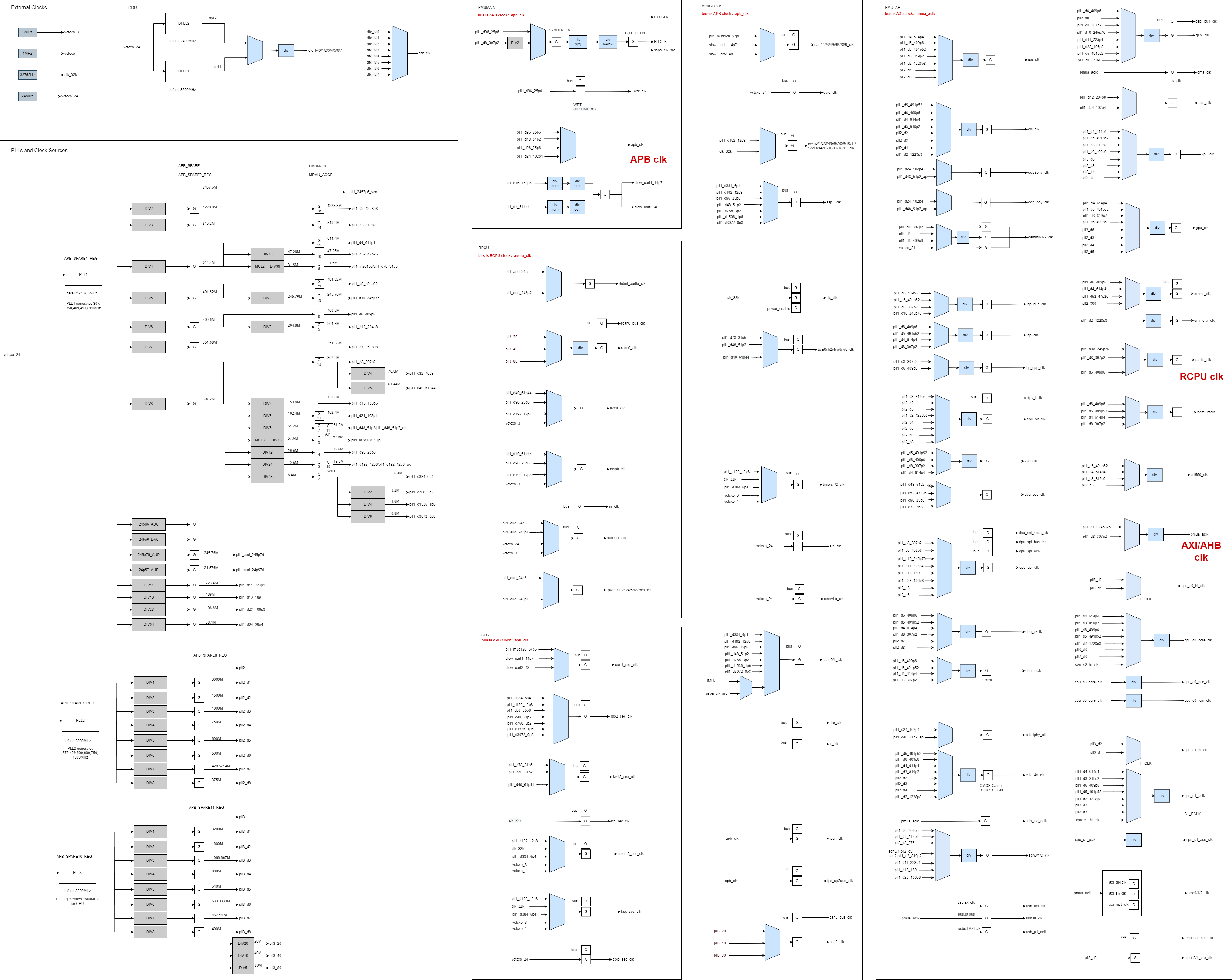
On Fri, Feb 21, 2025 at 03:10:46PM -0600, Alex Elder wrote:
> On 2/16/25 5:34 AM, Haylen Chu wrote:
> > On Thu, Feb 13, 2025 at 10:04:10PM -0600, Alex Elder wrote:
> > > On 1/3/25 3:56 PM, Haylen Chu wrote:
> > > > The clock tree of K1 SoC contains three main types of clock hardware
> > > > (PLL/DDN/MIX) and is managed by several independent controllers in
> > > > different SoC parts (APBC, APBS and etc.), thus different compatible
> > > > strings are added to distinguish them.
> > > >
> > > > Some controllers may share IO region with reset controller and other low
> > > > speed peripherals like watchdog, so all register operations are done
> > > > through regmap to avoid competition.
> > > >
> > > > Signed-off-by: Haylen Chu <heylenay@xxxxxxx>
> > >
> > > This is a really big patch (over 3000 lines), and a fairly large
> > > amount of code to review.  But I've given it a really thorough
> > > read and I have a *lot* of review comments for you to consider.
> >
> > Thanks for the detailed review!
> >
> > > First, a few top-level comments.
> > > - This driver is very comprehensive.  It represents essentially
> > >    *all* of the clocks in the tree diagram shown here:
> > > https://developer.spacemit.com/resource/file/images?fileName=DkWGb4ed7oAziVxE6PIcbjTLnpd.png
> > >    (I can tell you what's missing but I don't think it matters.)
> > > - In almost all cases, the names of the clocks match the names
> > >    shown in that diagram, which is very helpful.
> > > - All of the clocks are implemented using "custom" clock
> > >    implementations.  I'm fairly certain that almost all of
> > >    them can use standard clock framework types instead
> > >    (fixed-rate, fixed-factor, fractional-divider, mux, and
> > >    composite).  But for now I think there are other things
> > >    more important to improve.
> >
> > These three types of clocks are originally adapted from the vendor
> > driver, although the mix type has been largely rewritten during the
> > revisions.
> >
> > If the custom types don't cause big problems, I'd like to see the driver
> > merged first and we can gradually convert them to the more general ones,
> > which avoids blocking other SoC drivers.
>
> Understood.  Actually I have some other input that suggests
> repreenting things differently, but let me respond to your
> message (this one) first.
>
> . . .
>
> > > What do APBS, MPMU, APBC, and APMU stand for and represent?
> >
> > APMU and MPMU are abbreviated from Application/Main Power Management
> > Unit, as mentioned earlier in my reply to the dt-binding things. APBC
> > means APB Bus Clock Unit. APBS stands for APB SPARE and I'm not sure
> > about the precise meaning.
> >
> > These information seems important but I'm not sure about where they
> > should be documented. I could mention it in the cover letter or commit
> > message in next version.
>
> I guess knowing what they stand for is something, but knowing
> why they're separated and what function each plays is more
> important.  Don't worry about this for now.
>
> > > It seems each has its own clock controller, but can you
> > > offer any explanation about why they're divided that way?
> >
> > Sadly no, I have no idea why the clock bits are divided into several
> > MMIO regions, which really complicates binding.
>
> . . .
>
> > > > +/* APMU register offset */
> > > > +#define APMU_CCI550_CLK_CTRL		0x300
> > > > +#define APMU_CPU_C0_CLK_CTRL		0x38C
> > > > +#define APMU_CPU_C1_CLK_CTRL		0x390
>
> I didn't notice previously, but the above three are also
> duplicated a little later.
>
> > > > +#define APMU_JPG_CLK_RES_CTRL		0x20
> > > > +#define APMU_CSI_CCIC2_CLK_RES_CTRL	0x24
> > > > +#define APMU_ISP_CLK_RES_CTRL		0x38
> > > > +#define APMU_LCD_CLK_RES_CTRL1		0x44
> > > > +#define APMU_LCD_SPI_CLK_RES_CTRL	0x48
> > > > +#define APMU_LCD_CLK_RES_CTRL2		0x4c
> > > > +#define APMU_CCIC_CLK_RES_CTRL		0x50
> > > > +#define APMU_SDH0_CLK_RES_CTRL		0x54
> > > > +#define APMU_SDH1_CLK_RES_CTRL		0x58
> > > > +#define APMU_USB_CLK_RES_CTRL		0x5c
> > > > +#define APMU_QSPI_CLK_RES_CTRL		0x60
> > >
> > > APMU_USB_CLK_RES_CTRL is duplicated below.
> >
> > Thanks, will remove one along with other duplication.
> >
> > For the unused offsets, I prefer to keep the documented ones for future
> > completion of the driver. I don't think it's a large burden.
>
> That's fine.  Almost everything is used, so it does no real
> harm to include the few that aren't (yet).
>
> > > > +#define APMU_USB_CLK_RES_CTRL		0x5c
> > > > +#define APMU_DMA_CLK_RES_CTRL		0x64
> > > > +#define APMU_AES_CLK_RES_CTRL		0x68
> > > > +#define APMU_VPU_CLK_RES_CTRL		0xa4
> > > > +#define APMU_GPU_CLK_RES_CTRL		0xcc
> > > > +#define APMU_SDH2_CLK_RES_CTRL		0xe0
>
> . . .
>
> > > I'm going to say more about this below, but these definitions can
> > > be simplified a lot.  For example, the first one could be:
> > > 	CCU_PLL_RATE(2457600000UL, 0x0050dd64, 0x330ccccd),
> > >
> > > > +static const struct ccu_pll_rate_tbl pll1_rate_tbl[] = {
> > > > +	CCU_PLL_RATE(2457600000UL, 0x64, 0xdd, 0x50, 0x00, 0x33, 0x0ccccd),
> > > > +};
> > > > +
> > > > +static const struct ccu_pll_rate_tbl pll2_rate_tbl[] = {
> > > > +	CCU_PLL_RATE(3000000000UL, 0x66, 0xdd, 0x50, 0x00, 0x3f, 0xe00000),
> > > > +};
> > > > +
> > > > +static const struct ccu_pll_rate_tbl pll3_rate_tbl[] = {
> > > > +	CCU_PLL_RATE(3000000000UL, 0x66, 0xdd, 0x50, 0x00, 0x3f, 0xe00000),
> > > > +	CCU_PLL_RATE(3200000000UL, 0x67, 0xdd, 0x50, 0x00, 0x43, 0xeaaaab),
> > > > +	CCU_PLL_RATE(2457600000UL, 0x64, 0xdd, 0x50, 0x00, 0x33, 0x0ccccd),
> > > > +};
> > > > +
> > >
> > > Therre are only three PLL clocks, defined next.  All share the same
> > > lock register offset (MPMU_POSR), so that could be factored out.
> >
> > I'm not sure how to factor the offset out, could you please explain more
> > about it? By coding the offset in the macro or something else?
> >
> > I'd like to keep it as is, since PLL status in future SpacemiT SoCs are
> > likely to locate in different registers. Factoring the offset out won't
> > save a lot of characters, either.
>
> Keep it the way you have it.  Factoring it out doesn't help much.
>
> > > > +static CCU_PLL_DEFINE(pll1, "pll1", pll1_rate_tbl,
> > > > +		      APB_SPARE1_REG, APB_SPARE2_REG, APB_SPARE3_REG,
> > > > +		      MPMU_POSR, POSR_PLL1_LOCK, CLK_SET_RATE_GATE);
>
> . . .
>
> > > The next clock is weird, and it's the only one of its kind.  It is not
> > > represented in the clock tree diagram. It is a "factor 1" clock (so it
> > > just passes the parent's rate through), and has no gate.  Do you know
> > > why it's defined?  It is used only as one of the MPMU parent clocks.
> > > Why isn't just the pll1_d7 clock used in its place?
> >
> > It is represented in the diagram. The photo version of the diagram seems
> > hard to search so I will ask the vendor to publish a PDF version if
> > possible.
> >
> > As the definition involves no hardware bits, I guess it's actually an
> > alias listed to keep the tree structure in similar form. Will confirm
> > this with the vendor.
>
> This is what I meant by "not represented in the diagram."  It seems
> like it's just a place holder, more or less.  I think this is the
> only one defined here that's like that.

Yes, it's really a placeholder, as confirmed in another reply sent
earlier. Will remove it in the next version.

> > > > +static CCU_FACTOR_DEFINE(pll1_d7_351p08, "pll1_d7_351p08", CCU_PARENT_HW(pll1_d7),
> > > > +			 1, 1);
>
> . . .
>
> > > > +static struct ccu_ddn_tbl slow_uart1_tbl[] = {
> > > > +	{ .num = 125, .den = 24 },
> > > > +};
> > > > +static struct ccu_ddn_tbl slow_uart2_tbl[] = {
> > > > +	{ .num = 6144, .den = 960 },
> > > > +};
> > >
> > > I'll note here that this "slow_uart" gate is defined separately
> > > from the two slow UART DDN clocks below.  That's different from
> > > some other gated clocks.
> >
> > "slow_uart" is a gate that controlls both slow_uart1_14p7 and
> > slow_uart2_48. Enabling any one of these two clocks requires slow_uart
> > to ungate.
> >
> > I didn't find a good method to describe the structure under CCF (I'm
> > really new to it), thus listed it out and applied the CLK_IGNORE_UNUSED
> > trick. Any suggesions on this will be appreciated, thanks.
>
> Right now I have no suggestions.  Let's see the next version
> of the patches and we can maybe revisit this.

Okay.

> > > > +static CCU_GATE_DEFINE(slow_uart, "slow_uart", CCU_PARENT_NAME(osc),
> > > > +		       MPMU_ACGR,
> > > > +		       BIT(1), BIT(1), 0, CLK_IGNORE_UNUSED);
> > >
> > > What follows are the only two DDN clocks defined.  Both define
> > > a "table" of numerator/denominator pairs, but in both cases,
> > > the table has only one entry.
> > >
> > > Given that, why not simply encode the numerator and denominator
> > > in the ccu_info structure for each of these DDN clock instances?
> >
> > DDN types are M/N clocks, just like clk-fractional-divider. Hardcoded
> > tables (even with only one entry) work because their only consumers are
> > UARTs, which require a relatively fixed frequency. This will prevent us
> > from generating precise clock if we want the UART to operate under a
> > different baudrate.
> >
> > I'll cover more about this later.
>
> My point was that there's no need to define a "table" if there's
> only one entry.

You're right. I've decided to rewrite the DDN part in next version,
eliminating these tables or any type of hard-coded configuration.

> > > > +static CCU_DDN_DEFINE(slow_uart1_14p74, "slow_uart1_14p74", pll1_d16_153p6,
> > > > +		      &uart_ddn_mask_info, slow_uart1_tbl,
> > > > +		      MPMU_SUCCR, 0);
> > > > +static CCU_DDN_DEFINE(slow_uart2_48, "slow_uart2_48", pll1_d4_614p4,
> > > > +		      &uart_ddn_mask_info, slow_uart2_tbl,
> > > > +		      MPMU_SUCCR_1, 0);
> > > > +
> > > > +static CCU_GATE_DEFINE(wdt_clk, "wdt_clk", CCU_PARENT_HW(pll1_d96_25p6),
> > > > +		       MPMU_WDTPCR,
> > > > +		       BIT(1), BIT(1), 0x0,
> > > > +		       0);
> > > > +
> > >
> > > I couldn't find the "ripc_clk" on the clock tree diagram.  It is
> > > never used elsewhere, so I think this definition can go away.
> >
> > I'm not sure whether the ripc_clk doesn't exist or it's just missing in
> > both datasheet and clock tree diagram. Will confirm with the vendor.
> >
> > > > +static CCU_GATE_DEFINE(ripc_clk, "ripc_clk", CCU_PARENT_NAME(vctcxo_24m),
> > > > +		       MPMU_RIPCCR,
> > > > +		       0x3, 0x3, 0x0,
> > > > +		       0);
> > > > +
> > > > +static CCU_GATE_FACTOR_DEFINE(i2s_sysclk, "i2s_sysclk", CCU_PARENT_HW(pll1_d16_153p6),
> > > > +			      MPMU_ISCCR,
> > > > +			      BIT(31), BIT(31), 0x0, 50, 1,
> > > > +			      0);
> > > > +static CCU_GATE_FACTOR_DEFINE(i2s_bclk, "i2s_bclk", CCU_PARENT_HW(i2s_sysclk),
> > > > +			      MPMU_ISCCR,
> > > > +			      BIT(29), BIT(29), 0x0, 1, 1,
> > > > +			      0);
> > > > +
> > > > +static const struct clk_parent_data apb_parents[] = {
> > > > +	CCU_PARENT_HW(pll1_d96_25p6),
> > > > +	CCU_PARENT_HW(pll1_d48_51p2),
> > > > +	CCU_PARENT_HW(pll1_d96_25p6),
> > > > +	CCU_PARENT_HW(pll1_d24_102p4),
> > > > +};
> > > > +static CCU_MUX_DEFINE(apb_clk, "apb_clk", apb_parents,
> > > > +		      MPMU_APBCSCR,
> > > > +		      0, 2,
> > > > +		      0);
> > > > +
> > >
> > > The following clock is just called "wdt_clk" on the clock tree diagram.
> >
> > They're different things. The wdt_clk is defined a few lines earlier and
> > acts as the function clock of watchdog. Instead, wdt_bus_clk is its bus
> > clock.
> >
> > Most bus clocks in the clock tree diagram aren't listed explicitly, but
> > represented as a gate besides the function clock.
>
> OK, this is good to know.  Thank you.
>
> >
> > > > +static CCU_GATE_DEFINE(wdt_bus_clk, "wdt_bus_clk", CCU_PARENT_HW(apb_clk),
> > > > +		       MPMU_WDTPCR,
> > > > +		       BIT(2), BIT(2), 0x0,
> > > > +		       0);
> >
> > I do find a typo here. BIT(0) should be used here instead of BIT(2),
> > which is the reset bit for watchdog.
> >
> > > > +/*	MPMU clocks end		*/
> > > > +
> > > > +/*	APBC clocks start	*/
> > > > +static const struct clk_parent_data uart_clk_parents[] = {
> > > > +	CCU_PARENT_HW(pll1_m3d128_57p6),
> > > > +	CCU_PARENT_HW(slow_uart1_14p74),
> > > > +	CCU_PARENT_HW(slow_uart2_48),
> > > > +};
> > >
> > > I might be misunderstanding this, but all of the 9 UART clocks below
> > > share a common gate.
> >
> > AFAIK they don't share the common gate. Each uart comes with its own
> > functional gate, bus gate and multiplexer. The diagram seems a little
> > confusing: only one gate is drawn to avoid duplication.
>
> OK this is also good to know, thanks.
>
> > This applies for PWM as well. There're 10 different UART clock/reset
> > registers, each contains a gate bit for functional clock and one for
> > bus clock,  confirming the idea[1].
> >
> > > I *think* that gate should be represented as a distinct clock so that
> > > it can be properly reference-counted. There are numerous cases of this.
>
> After I sent this I concluded the above statement was wrong.
>
> > > Also note there is no uart1 clock; I think the clock tree diagram
> > > erroneously calls the first clock "uart1" (not uart0).
> >
> > The clocks are reordered to match our current devicetree, where the
> > first uart is uart0 and uart1 is assigned to the one in RCPU (real-time
> > CPU) region.
>
> I guess what I care about is that it is done in a way that avoids
> any confusion.  I believe what you describe makes sense.
>
> > > > +static CCU_MUX_GATE_DEFINE(uart0_clk, "uart0_clk", uart_clk_parents,
> > > > +			   APBC_UART1_CLK_RST,
> > > > +			   4, 3, BIT(1), BIT(1), 0x0,
> > > > +			   CLK_IS_CRITICAL);
>
> . . .
>
> > > Here we begin a bunch of definitions of "bus clocks".  They are all
> > > simply gates, and the clock tree diagram shows these paired with
> > > another gated parent.
> >
> > Please note in the diagram, the clock beside the bus clock isn't the
> > parent of the bus clock. Without special notes, all bus clocks in the
> > APBC region take apb_clk as parent. All bus clocks in the APMU region
> > take pmua_aclk as parent.
>
> OK, I think there might be a note at the top of the diagram
> that suggests this, but I'm very happy to have you explain it
> to me.
>
> > > This says to me that in order to use a "child clock" in this
> > > situation, both the "regular gate" and the "bus gate" clock must be
> > > defined, and a reference to it taken (with clk_get() or similar).
> >
> > No, functional clock and bus clock are completely irrelevant. They
> > control different parts of a peripheral. Taking UART as example, you do
> > need to take both function and bus clock for normal operation; but if
> > the bus clock is disabled, the UART could continue to send data. Only
> > the bus component won't work and the registers couldn't be accessed.
>
> The bus clocks sound like interconnects.  But I'm not going to
> even go there right now...
>
> > > Can you confirm this?
> > > > +
>
> . . .
>
> > > The next two parent clocks are duplicates.  It looks this way on the
> > > clock tree diagram as well.  Is this correct? Can you find out from
> > > SpacemiT whether one of them is actually a different clock (like
> > > pll2_d6 or something)?  It makes no sense to have two multiplexed
> > > parent clocks with the same source.
> >
> > Yes, will confirm it later. The register description[2] suggests it's
> > wrong (there aren't two configuration for MIPI_BIT_CLK_SEL resulting in
> > the same frequency).
> >
> > > > +	CCU_PARENT_HW(pll2_d8),
> > > > +	CCU_PARENT_HW(pll2_d8),
> > > > +};
>
> OK thank you.

This has been confirmed in the earlier message as well, the duplicated
parents ARE wrong. Thanks for pointing this out.

> > > > +static CCU_DIV_FC_MUX_GATE_DEFINE(dpu_bit_clk, "dpu_bit_clk", dpubit_parents,
> > > > +				  APMU_LCD_CLK_RES_CTRL1,
> > > > +				  17, 3, BIT(31),
> > > > +				  20, 3, BIT(16), BIT(16), 0x0,
> > > > +				  0);
>
> . . .
>
> > > > +static CCU_DIV_FC_MUX_GATE_DEFINE(sdh1_clk, "sdh1_clk", sdh01_parents,
> > > > +				  APMU_SDH1_CLK_RES_CTRL,
> > > > +				  8, 3, BIT(11),
> > > > +				  5, 3, BIT(4), BIT(4), 0x0,
> > > > +				  0);
> > >
> > > This is strange too.  sdh2_parents is identical to sdh01_parents.
> >
> > No, it isn't. pll2_d5 is a parent for sdh0/1; for sdh2, pll1_d3_819p2
> > replaces it.
>
> I see that now in the code, but not in the diagram.
> I guess I'll assume the code is right.
>
> > > All of the bits used are identical for the three control registers.
> > > The clock tree diagram shows all three of these sdhx clocks sharing
> > > a single parent mux.  Why is sdh2_parents defined separately?
> >
> > I don't think the mux is shared. It should be the same case for
> > UART/PWM clocks, as described earlier.
>
> I'm sure you're right.
>
> > > > +static const struct clk_parent_data sdh2_parents[] = {
> > > > +	CCU_PARENT_HW(pll1_d6_409p6),
> > > > +	CCU_PARENT_HW(pll1_d4_614p4),
> > > > +	CCU_PARENT_HW(pll2_d8),
> > > > +	CCU_PARENT_HW(pll1_d3_819p2),
> > > > +	CCU_PARENT_HW(pll1_d11_223p4),
> > > > +	CCU_PARENT_HW(pll1_d13_189),
> > > > +	CCU_PARENT_HW(pll1_d23_106p8),
> > > > +};
>
> . . .
>
> > > You could reduce some duplication here using a simple
> > > macro for defining the address of the clk_hw structure:
> > >
> > > #define CLK_HW(x)	&x.common.hw
> > >
> > > (Add parentheses if you like.)  It saves 3 characters for
> > > each clock...
> >
> > Looks good to me, but
>
> Don't bother for now.  It can be fixed easily later if
> it's important.

Thanks.

> > > > +static struct clk_hw_onecell_data k1_ccu_apbs_clks = {
> > > > +	.hws = {
> > > > +		[CLK_PLL1]		= &pll1.common.hw,
> > > > +		[CLK_PLL2]		= &pll2.common.hw,
> > > > +		[CLK_PLL3]		= &pll3.common.hw,
> > > > +		[CLK_PLL1_D2]		= &pll1_d2.common.hw,
> > > > +		[CLK_PLL1_D3]		= &pll1_d3.common.hw,
> > > > +		[CLK_PLL1_D4]		= &pll1_d4.common.hw,
> > > > +		[CLK_PLL1_D5]		= &pll1_d5.common.hw,
> > > > +		[CLK_PLL1_D6]		= &pll1_d6.common.hw,
> > > > +		[CLK_PLL1_D7]		= &pll1_d7.common.hw,
> > > > +		[CLK_PLL1_D8]		= &pll1_d8.common.hw,
> > > > +		[CLK_PLL1_D11]		= &pll1_d11_223p4.common.hw,
> > > > +		[CLK_PLL1_D13]		= &pll1_d13_189.common.hw,
> > > > +		[CLK_PLL1_D23]		= &pll1_d23_106p8.common.hw,
> > > > +		[CLK_PLL1_D64]		= &pll1_d64_38p4.common.hw,
> > > > +		[CLK_PLL1_D10_AUD]	= &pll1_aud_245p7.common.hw,
> > > > +		[CLK_PLL1_D100_AUD]	= &pll1_aud_24p5.common.hw,
> > > > +		[CLK_PLL2_D1]		= &pll2_d1.common.hw,
> > > > +		[CLK_PLL2_D2]		= &pll2_d2.common.hw,
> > > > +		[CLK_PLL2_D3]		= &pll2_d3.common.hw,
> > > > +		[CLK_PLL2_D4]		= &pll2_d4.common.hw,
> > > > +		[CLK_PLL2_D5]		= &pll2_d5.common.hw,
> > > > +		[CLK_PLL2_D6]		= &pll2_d6.common.hw,
> > > > +		[CLK_PLL2_D7]		= &pll2_d7.common.hw,
> > > > +		[CLK_PLL2_D8]		= &pll2_d8.common.hw,
> > > > +		[CLK_PLL3_D1]		= &pll3_d1.common.hw,
> > > > +		[CLK_PLL3_D2]		= &pll3_d2.common.hw,
> > > > +		[CLK_PLL3_D3]		= &pll3_d3.common.hw,
> > > > +		[CLK_PLL3_D4]		= &pll3_d4.common.hw,
> > > > +		[CLK_PLL3_D5]		= &pll3_d5.common.hw,
> > > > +		[CLK_PLL3_D6]		= &pll3_d6.common.hw,
> > > > +		[CLK_PLL3_D7]		= &pll3_d7.common.hw,
> > > > +		[CLK_PLL3_D8]		= &pll3_d8.common.hw,
> > > > +		[CLK_PLL3_80]		= &pll3_80.common.hw,
> > > > +		[CLK_PLL3_40]		= &pll3_40.common.hw,
> > > > +		[CLK_PLL3_20]		= &pll3_20.common.hw,
> > > > +
> > > > +	},
> > > > +	.num = CLK_APBS_NUM,
> > >
> > > It sure would be nice to be able to use ARRAY_SIZE() here but
> > > alas I don't think it's possible here.
> >
> > CLK_*_NUM will be removed in the next revision, as it's actually not a
> > binding. I'm looking for a better way to represent these clocks.
> >
> > Maybe represent the clocks with (ID, struct clk_hw *) pairs and
> > generate struct clk_hw_onecell_data dynamically during probe.
>
> Yes I think I have a suggestion but I'll hold off until I send
> out another message in which I suggest something different.
>
> > > > +};
>
> . . .
>
> > > The only time the "PLL lock" is needed is with PLL clocks.  Can you
> > > encode this flag, or perhaps the address of the lock register,
> > > into the ccu_pll structure instead somehow?
> > >
> > > If so you wouldn't need this spacemit_ccu_data structure, and could
> > > simply use the clk_hw_onecell_data structure in its place.
> >
> > We could scan the clk_hw_onecell_data array before the probing, but I
> > don't think it's worth.
> >
> > As the raw clk_hw_onecell_data is likely to be removed in the next
> > revision, I'll try to avoid the flag during refactoring.
>
> I think you'll be able to.
>
> > > > +struct spacemit_ccu_data {
> > > > +	struct clk_hw_onecell_data *hw_clks;
> > > > +	bool need_pll_lock;
> > > > +};
>
> . . .
>
> > > The next two pointers are regmap pointers.  Could the
> > > name of the fields suggest that?  (They sound like raw
> > > memory addresses to me.)
> >
> > Do "common.regmap" and "common.lock_regmap" sound better for you?
>
> Yes I think that's an improvement.
>
> > > > +		common->base		= priv->base;
> > > > +		common->lock_base	= priv->lock_base;
>
> . . .
>
> > > > +		ret = devm_clk_hw_register(dev, hw);
> > > > +		if (ret) {
> > > > +			dev_err(dev, "Cannot register clock %d - %s\n",
> > > > +				i, name);
> > >
> > > Just use hw->init->name here instead of name.
> >
> > Will change in the next version.
>
> . . .
>
> > > You allocate the priv structure, but never free it (a bug).
> > > It only holds 3 values; just pass them as arguments when
> > > registering the CCU, as suggested above.
> >
> > The allocation is done through a devres variant, it should be released
> > automatically. Please correct me if I'm wrong.
>
> You're right.  But my other point about priv being unnecessary
> (just pass the three values as arguments) remains.

Makes sense to me, I'll drop the structure.

> > > > +	priv = devm_kzalloc(dev, sizeof(*priv), GFP_KERNEL);
> > > > +	if (!priv)
> > > > +		return -ENOMEM;
>
> . . .
>
> > > End of "ccu-k1.c"!!!
> >
> > It's really a lot of lines lol
> >
> > > > diff --git a/drivers/clk/spacemit/ccu_common.h b/drivers/clk/spacemit/ccu_common.h
> > > > new file mode 100644
> > > > index 000000000000..242461ee592f
> > > > --- /dev/null
> > > > +++ b/drivers/clk/spacemit/ccu_common.h
> > > > @@ -0,0 +1,51 @@
>
> . . .
>
> > > Although I think the following macros are nice and concise, they
> > > obscure the fact that they're essentially renaming existing
> > > regmap operations.  They don't really add much value; the
> > > regmap functions are pretty clear.
> >
> > They're just for saving some characters,
> >
> > 	regmap_read(common->base, common->reg_ctrl, &tmp)
> >
> > is much longer than
> >
> > 	ccu_read(common, ctrl, &tmp)
> >
> > Of course it could be changed, if you're still strongly against it,
>
> It's OK for now, but I might make the same suggestion in a future
> version of the series.

Okay, then will keep it as it, at least for now.

> > > Although regmap_read() returns a value, you never check for an
> > > error when calling ccu_read().
> >
> > I don't expect that access to a MMIO regmap could fail. There shouldn't
> > be any cases of failure, so I don't check it.
> >
> > > > +#define ccu_read(reg, c, val)	regmap_read((c)->base, (c)->reg_##reg, val)
>
> It should never return an error.  But what if it did?  I'm
> mainly thinking about the very first attempt to read from
> the I/O space.  It's probably OK; lots of existing code
> ignores any return value from regmap_read.
>
> . . .
>
> > > > diff --git a/drivers/clk/spacemit/ccu_ddn.c b/drivers/clk/spacemit/ccu_ddn.c
> > > > new file mode 100644
> > > > index 000000000000..1df555888ecb
> > > > --- /dev/null
> > > > +++ b/drivers/clk/spacemit/ccu_ddn.c
>
> . . .
>
> > > The next three functions are never used and can be removed.
> > >
> > > The reason is that the only time they'd be used is when
> > > CCU_DDN_GATE_DEFINE() (defined in "ccu_ddn.h") is called,
> > > but it never is.  So you can get rid of CCU_DDN_GATE_DEFINE(),
> > > and once you do that there's no need for ccu_ddn_disable(),
> > > ccu_ddn_enable(), and ccu_ddn_is_enabled().  Furthermore,
> > > these three functions are the only place the "reg_sel"
> > > field in the ccu_common structure is used, and without
> > > these functions, that field serves no purpose.  So that
> > > field can go away, and there's no need to provide a value
> > > for initializing it in all those clock definition macros.
> >
> > When cleaning up the driver from the vendor source, I tried to keep most
> > clock types included since future SpacemiT SoCs made may make use of
> > them. It seems too farsighted as this patch is already quite large.
> >
> > I'll remove the unused clock types as well as the reg_sel field, thanks.
>
> This is good practice.  Don't add code that you expect
> to use at a future date.  Keep that out, and add it in
> *when* you need it.  Otherwise it's basically dead code.
>
> . . .
>
> > > I'm going to say more about this below, but I think the
> > > factor can be removed and hard-coded here.
> >
> > Alright, we could hardcode it for now to make the patch as simple as
> > possible. If different factors are used in future SoCs, it isn't hard
> > to add it back later.
>
> Exactly.
>
> > > > +		rate = (*prate * params->tbl[i].den) /
> > > > +			(params->tbl[i].num * params->info->factor);
> > >
>
> . . .
>
> > > Here is a general comment that applies to a bunch of places in
> > > this code.  You can concisely define a field with a single
> > > mask value.  That means there is no need to define both a mask
> > > (or a field width) and a shift.  What you need is defined in
> > > <linux/bitfield.h>.  There you will find a set of macros
> > > like FIELD_GET() and FIELD_PREP(), or alternatively a set
> > > of inline functions like u32_get_bits() and u32_encode_bits().
> >
> > I think both macros and inline functions in bitfield.h work with only
> > constant masks. With non-constant masks, some checks cannot be optimized
> > out, resulting in compilation errors.
>
> Yes, this was true some time back and I suppose it still is.
> For some reason I thought there might have been a way to use
> non-constant masks.  Anyway, I still think something similar
> to u32_get_bits() or FIELD_GET() is nicely encapsulated and
> less error-prone than "manually" shifting and masking.
>
> Don't worry about it for now, but again I might suggest it
> again.
>
> > > > +	unsigned int num_mask;
> > > > +	unsigned int den_mask;
> > > > +	unsigned int num_shift;
> > > > +	unsigned int den_shift;
> > > > +};
>
> . . .
>
> > > > diff --git a/drivers/clk/spacemit/ccu_mix.c b/drivers/clk/spacemit/ccu_mix.c
> > > > new file mode 100644
> > > > index 000000000000..b46eeb59faea
> > > > --- /dev/null
> > > > +++ b/drivers/clk/spacemit/ccu_mix.c
>
> . . .
>
> > > > +static int ccu_mux_set_parent(struct clk_hw *hw, u8 index)
> > > > +{
> > > > +	struct ccu_mix *mix = hw_to_ccu_mix(hw);
> > > > +	struct ccu_common *common = &mix->common;
> > > > +	struct ccu_mux_config *mux = mix->mux;
> > > > +	int ret = 0;
> > > > +	u32 mask;
> > > > +
> > > > +	if (mux->table)
> > >
> > > You should verify that the index is less than the
> > > number of entries in the table before you blindly
> > > dereference it here.
> >
> > The desired index is found by searching in clk_fetch_parent_index(),
> > thus is always be valid, isn't it?
> >
> > However, this is a dead codepath: no clock hardware comes with a valid
> > table. The whole if could be removed for simplication.
>
> That's even better.
>
> > > > +		index = mux->table[index];
>
> . . .
>
> > > > +	u32 val_enable;
> > > > +	u32 val_disable;
> > > > +	u32 flags;
> > >
> > > When you have a flags field like this, it's helpful to add a comment
> > > that indicates what values it can take on.  I believe in all cases
> > > like this, the flags values are standard clock framework flags.
> >
> > Yes.
> >
> > > So what I mean is do something like this:
> > >
> > >      u32 flags;		/* E.g., CLK_IGNORE_UNUSED */
> >
> > Do you think
> >
> > 	u32 flags;		/* standard CCF flags */
> >
> > ls more descriptive?
>
> No, but your way is OK.

Thanks.

> >
> > > > +};
>
> . . .
>
> > > > +#define CCU_GATE_DEFINE(_struct, _name, _parent, _reg, _gate_mask,		\
> > > > +			 _val_enable, _val_disable, _flags)			\
> > >
> > > There is one case where the _flags value is CLK_IGNORE_UNUSED, and
> > > one case where it is CLK_IS_CRITICAL.
> >
> > The UART0 (booting UART) and all core clocks are marked as
> > CLK_IS_CRTICAL, not just one case.
> >
> > > All others pass 0.  Given
> > > that, you could define two macros and remove the 0 argument from
> > > most of the callers:
> >
> > I'd like to always keep the flags field, since keeping the clock
> > definitions intact and in the same format helps reading. There're a
> > bunch of clocks.
>
> OK.
>
> . . .
>
> > > I'd put the "2" somewhere else in the name of this.  It suggests
> > > "divide by two" but it's really a "second DIV_FC_MUX_GATE" macro.
> >
> > Is DIV_SPLIT_FC_MUX_GATE a better name? The difference between this and
> > DIV_FC_MUX_GATE is that the fc bit locates in a different register.
>
> Either is fine.  My point was about "DIV2" suggesting "divide
> by two".
>
> . . .
>
> > > > diff --git a/drivers/clk/spacemit/ccu_pll.c b/drivers/clk/spacemit/ccu_pll.c
> > > > new file mode 100644
> > > > index 000000000000..81b929ca1c5c
> > > > --- /dev/null
> > > > +++ b/drivers/clk/spacemit/ccu_pll.c
>
> . . .
>
> > > > +	unsigned int i;
> > > > +
> > > > +	for (i = 0; i < params->tbl_size; i++) {
> > > > +		if (params->rate_tbl[i].rate <= rate) {
> > > > +			if (max_rate < params->rate_tbl[i].rate)
> > > > +				max_rate = params->rate_tbl[i].rate;
> > > > +		}
> > > > +	}
> > > > +
> > >
> > > I don't like that you're passing a compile-time defined
> > > frequency (which might not match reality).
> >
> > We could make the rate_tbl sorted, which should improve both set_rate
> > and round_rate a lot.
>
> That might be nice, but it's not strictly necessary.  But if you
> don't do that, fix the loop above.
>
> > > > +	return MAX(max_rate, PLL_MIN_FREQ);
> > > > +}
>
> . . .
>
> That's the end of my response.
>
> Now on to my bigger proposal.  Do *not* delay posting the
> next version of your series based on my next message.

Which one does "next message" refer to? Is it the one about dt-binding
designing, or should I wait for another message?

> Just send out an update that addresses all of the feedback
> you have received so far.  If my proposal makes sense we can
> talk about how to modify that next version to incorporate it.

Okay.

> Thanks.
>
> 					-Alex

Best regards,
Haylen Chu
